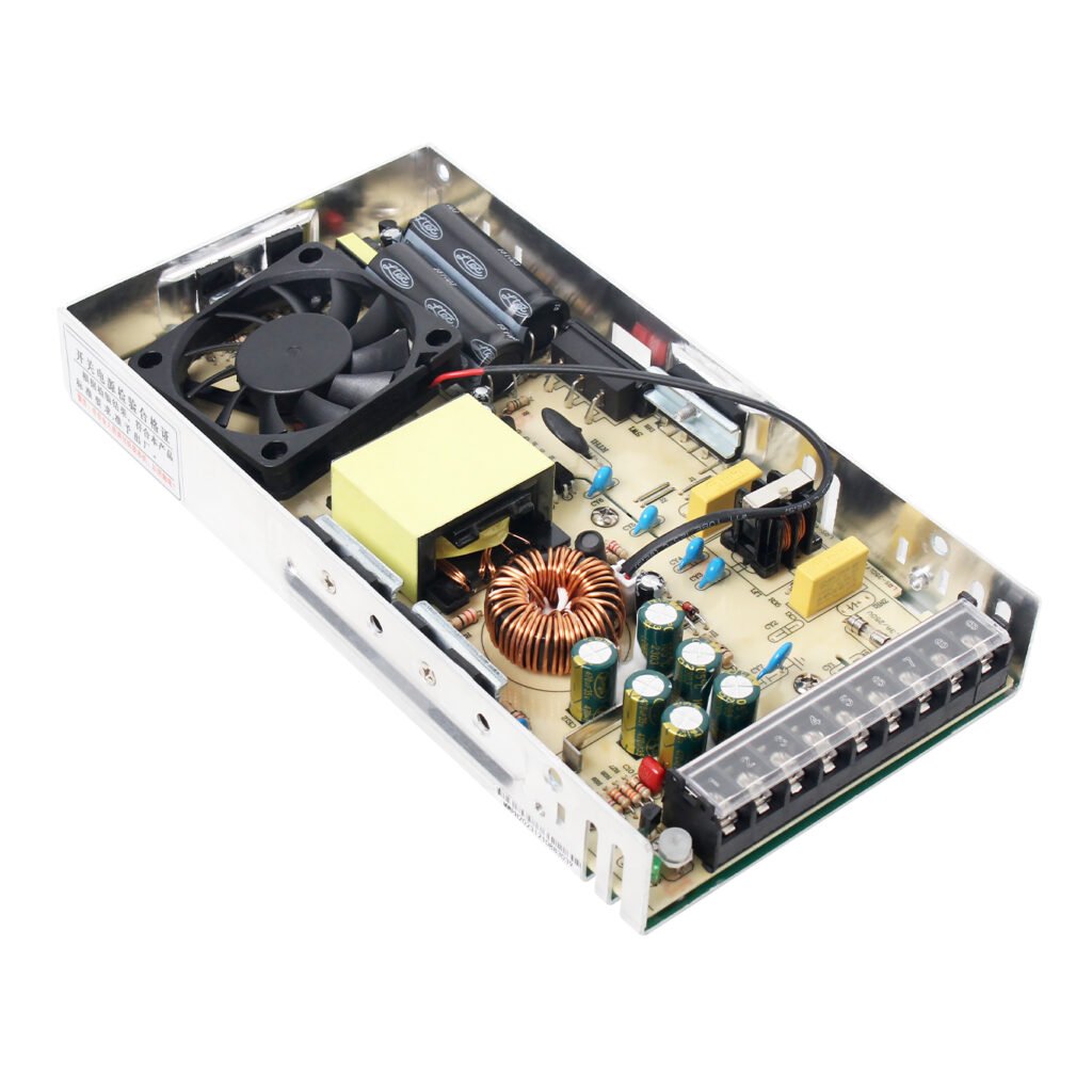
SMPS PCB Design (Switched Mode Power Supply PCB Design) is a complex and crucial process that involves multiple aspects to ensure the power supply’s performance, stability, and safety. Here are some key points to consider in SMPS PCB design:
I. Circuit Structure and Design Principles
- Understanding Circuit Operation and Characteristics:
- SMPS primarily consists of a main switching transistor, transformer, control circuitry, and filtering circuits.
- Before designing, thoroughly understand the function of each component and the overall circuit operation.
- Drawing a Complete Circuit Diagram:
- Follow a left-to-right drawing convention.
- Clearly indicate the source and destination of each sheet in a multi-sheet diagram, along with their respective positions.
- Mark critical sections or notes requiring special attention on the diagram.
- Use consistent component symbols to avoid confusion.
II. Noise Generation and Countermeasures
- Noise Generation Causes:
- SMPS, due to its high operating frequency (at least 20KHz and above) and square-wave voltage waveform, generates noise during rapid switching.
- Noise primarily stems from electrostatic and electromagnetic induction.
- Noise Countermeasures:
- EMI Filter Design: Keep the live wire smooth with minimal bends, use thick and short ground wires, position the EMI filter loop away from power transistors and transformers, and reduce the contact resistance between FG and the chassis.
- Layout Optimization: Keep high-current paths as short as possible to reduce loop area and radiation. Separate power and control circuits to minimize interference.
- Component Placement: Ensure power transistors’ heat sinks are independent and grounded. Position Snubbers close to their respective components. Strategically place the main transformer to reduce interference.
III. Production Considerations and Safety Standards
- Production Considerations:
- Standardize component orientations (polarity) such as diodes and electrolytic capacitors.
- Ensure component pin spacing meets production requirements.
- Choose heat sinks based on their cooling efficiency.
- Position special components for easy access during maintenance, such as power transistors and rectifier diodes.
- Consider production fixture needs, leaving space around the PCB edges.
- Safety Standards:
- Comply with safety standards specific to different countries or regions, such as UL (USA), VDE (Europe), CSA (Canada), etc.
IV. PCB Layout Techniques
- Optimal PCB Size: Determine the appropriate PCB size based on circuit complexity and component count.
- Trace Width and Spacing:
- Use narrow traces for high-impedance signals and wide traces for low-impedance signals.
- Determine trace spacing based on the maximum operating voltage difference between two traces.
- Component Distribution:
- Decide on the positions of all components, considering the needs of special-structure components.
- Arrange components to fit the PCB size, considering path lengths and connections.
- Avoid placing components too close to prevent magnetic and capacitive coupling effects.
V. Quality Control Techniques
- Inspection During Artwork Completion:
- Check PCB size, hole positions, gaps, trace widths, drill sizes, etc.
- Verify font size, polarity, pin positions, and other markings on the silkscreen layer.
- Ensure that PART NO, company logos, and other identifications are correctly placed.
- Inspection During Film Completion:
- Check film size for errors and ensure tolerances are within acceptable limits.
- Inspect for shadows, breaks, transparency issues, shorts, or pinholes.
VI. Additional Considerations
- Thermal Design: Plan for proper component and heat sink placement to ensure the power supply does not overheat during prolonged operation.
- EMC (Electromagnetic Compatibility) and EMI (Electromagnetic Interference): Ensure the design complies with relevant standards to prevent interference with surrounding equipment.
- Debugging and Testing: Adjust design parameters based on load characteristics and input power conditions during actual application. Conduct power-up performance, dynamic response, efficiency tests, and EMC tests to ensure stability and reliability.
In summary, SMPS PCB design is a comprehensive process requiring solid electronic theory knowledge and extensive practical experience. By implementing reasonable layouts, effective noise countermeasures, strict production and safety standards, and meticulous quality control techniques, one can design SMPS products with excellent performance, stability, and reliability.
